Highlighting the possibilities of PCB technology in the field of power electronic substrates
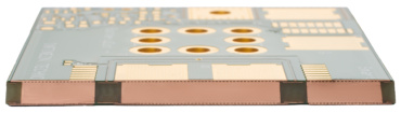
T. Gottwald, Director Next Generation Products , Dr. Manuel Martina, Christian Rößle of Schweizer Electronics’ The transition from mechanical to electrical power brings new challenges to manufacturers and requires new solutions for the electrical system, where the PCB (Printed Circuit Board) is of crucial importance. High currents, heat dissipation of power electronic components, low inductances and miniaturization needs are only a few of the requirements that lead to innovative solutions on PCB level.Chip embedding technologies are meanwhile used to embed thin bare dies of Power Semiconductors into the PCB which leads to powerful alternatives to conventional power electronic modules. Introduction The global warming and the pressure on CO2 reduction led to an increasing ratio of Renewable Energy from wind power plants and solar energy systems. As these sources must be connected to the power grid DC to AC, AC to DC, DC to DC converters and the like are applications of growing volume. Because the energy of renewable sources tends to be more costly, the total systems´ efficiency is crucial. Due to the same reason the Automotive Industry is under legislative pressure to achieve their CO2 reduction targets. That’s why hybrid and electrical drive is bringing momentum to the development of new solutions for the electrification of automotive applications. High power demand leads to increasing challenges for high current and for thermal management of dissipated power losses as well. The power conversion is done with power semiconductors which have to be assembled on a substrate. This can either be a power module made from Ceramic substrates like Direct Bonded Copper (DBC/DCB) or with a Printed Circuit Board (PCB). The task of the substrate is to manage high currents, high heat dissipation and high switching frequencies to support the electrical conversion of energy in the best way. Over the last few years PCBs achieved an increasing share in these applications as they typically have a cost advantage over Ceramics. PCBs offer the opportunity to manage the power stage and the control board in one single substrate while Ceramic power stages always need to have an additional control board and the related interconnection architecture like plugs and cables. This article highlights the possibilities of PCB technology in the field of power electronic substrates. Heavy copper PCBsHeavy copper PCBs have been used in the automotive industry for a long time, e.g. for fuse- and relay boxes. This technology experiences a revival as the electrical power increases in many applications. The technology is also useful to reduce the parasitic inductance of the conductors by using the heavy copper layers as power lines which can be stacked one above the other in a heavy copper multilayer. Up to 4 layers made from 400 µm (12 oz) Copper can be realized in the inner layers, which leads to a potential ampacity of more than 1000 A. The outer layers of such a heavy copper multilayer should be kept below 150 µm. Otherwise additional effort must be made for the solder mask process to achieve a safe electrical insulation. Fig. 1: 6-layer multilayer PCB with 4 inner layers, 400 µm copper each. Power Combi-BoardThe disadvantage of heavy copper PCB technology is the incompatibility with fine pitch structures which cannot be etched with heavy copper. Therefor a power electronic system typically consists of a power stage with heavy copper design and a separate control board with standard copper thickness for SMT assembly. The installation space must be large enough to host both boards and the connectors between the two boards.With the Power Combi Board, a combination of both requirements can be achieved. Heavy copper is partially installed in the inner layers besides standard copper construction. The electrical connection of the whole board is carried out with one common outer layer in SMT compatible copper thickness. Fig.2: Power Combi Board: Heavy copper besides standard copper thickness for power and control in one PCB For heat dissipation the insulation layer between the heavy copper layers are a barrier for optimal heat transportation in z-axis. Heavy copper PCB technology should therefor preferably be used to manage high currents. If heat dissipation is important for the application, other technologies should also be considered like the Inlay technology. Insulated Metal Substrates (IMS)An Insulated Metal Substrate typically consists of a metal heat sink, a thin insulation layer and a single copper layer on top. The construction is useful for simple designs which host a lot of heat generating components. For more complex components it is not possible to do the routing with one layer only.Today IMS substrates can also be manufactured with more than one layer to enable the combination of higher complexity layouts with optimized heat dissipation. Fig. 3: Insulated Metal substrate with copper backside The typical Aluminum backside is a light weight but also a high CTE metal. To increase the reliability of the assembled components Copper was introduced as heat sink metal on the back side. This also improves the thermal capacity and other characteristic as shown in Fig. 4 Fig.4: Comparison of characteristics Copper vs. Aluminum Inlay TechnologyFor minimizing the thermal resistance from the power components to the heat sink the shortest way will lead to the lowest thermal resistance. In most cases the heat is dissipated in z-axis from the assembled top side of a PCB through the board to a heat sink, which is installed at the bottom. By laminating a massive copper element into the PCB, the thermal resistance can be reduced dramatically. If the Inlay is not only used for heat dissipation but also for high currents the lowest ohmic resistance can also be achieved. Fig 5: Left: Cross section through an inlay board with 2 mm thick copper inlays in the inner structure. Right: Top and bottom side of an inlay board for 1200 A peak currents. Embedding TechnologyWhen it comes to highest performance requirements and lowest installation space, conventional solutions encounter limitations regarding installation space and power density. Miniaturization was the first driver for embedding because space savings are possible if some of